- 您现在的位置:买卖IC网 > Sheet目录377 > 2N7002E-7-F (Diodes Inc)MOSFET N-CH 60V 240MA SOT23-3
�� �
�
�2N7002E�
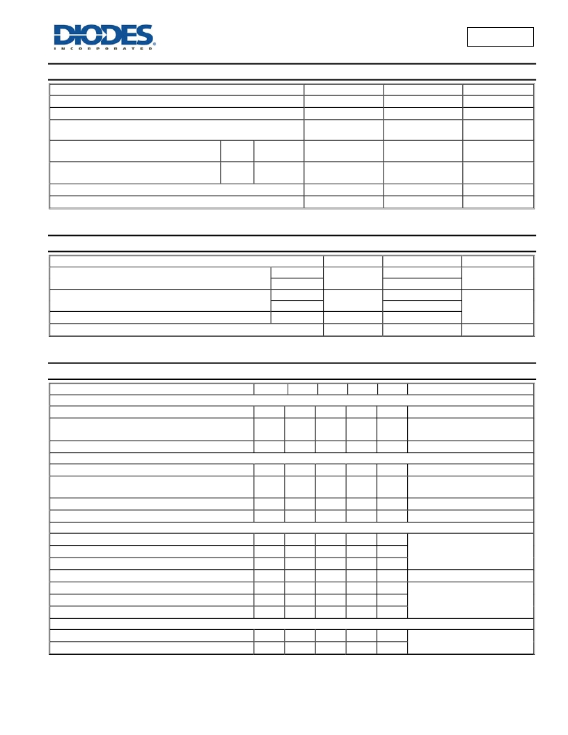
�Maximum� Ratings� (@T� A� =� +25°C,� unless� otherwise� specified.)�
�Characteristic�
�Drain-Source� Voltage�
�Drain-Gate� Voltage� R� GS� ?� 1.0M� ?�
�Symbol�
�V� DSS�
�V� DGR�
�Value�
�60�
�60�
�Units�
�V�
�V�
�Gate-Source� Voltage�
�Continuous�
�Pulsed�
�V� GSS�
�±20�
�±40�
�V�
�Continuous� Drain� Current� (Note� 5)� V� GS� =� 10V�
�Continuous� Drain� Current� (Note� 6)� V� GS� =� 10V�
�Maximum� Body� Diode� Forward� Current� (Note� 6)�
�Pulsed� Drain� Current� (10μs� pulse,� duty� cycle� =� 1%)�
�Steady�
�State�
�Steady�
�State�
�T� A� =� +25°C�
�T� A� =� +70°C�
�T� A� =� +25°C�
�T� A� =� +70°C�
�I� D�
�I� D�
�I� S�
�I� DM�
�250�
�200�
�300�
�240�
�500�
�800�
�mA�
�mA�
�mA�
�mA�
�Thermal� Characteristics� (@T� A� =� +25°C,� unless� otherwise� specified.)�
�Characteristic�
�Symbol�
�Value�
�Units�
�Total� Power� Dissipation�
�Thermal� Resistance,� Junction� to� Ambient�
�Thermal� Resistance,� Junction� to� Case�
�Operating� and� Storage� Temperature� Range�
�(Note� 5)�
�(Note� 6)�
�(Note� 5)�
�(Note� 6)�
�(Note� 6)�
�P� D�
�R� θ� JA�
�R� θ� JC�
�T� J,� T� STG�
�370�
�540�
�348�
�241�
�91�
�-55� to� 150�
�mW�
�°C/W�
�°C�
�Electrical� Characteristics� (@T� A� =� +25°C,� unless� otherwise� specified.)�
�Characteristic�
�Symbol�
�Min�
�Typ�
�Max�
�Unit�
�Test� Condition�
�OFF� CHARACTERISTICS� (Note� 7)�
�Drain-Source� Breakdown� Voltage�
�BV� DSS�
�60�
�70�
�?�
�V�
�V� GS� =� 0V,� I� D� =� 10μA�
�Zero� Gate� Voltage� Drain� Current�
�Gate-Body� Leakage�
�@� T� C� =� +25°C�
�@� T� C� =� +125°C�
�I� DSS�
�I� GSS�
�?�
�?�
�?�
�?�
�1.0�
�500�
�±10�
�μA�
�nA�
�V� DS� =� 60V,� V� GS� =� 0V�
�V� GS� =� ±15V,� V� DS� =� 0V�
�ON� CHARACTERISTICS� (Note� 7)�
�Gate� Threshold� Voltage�
�V� GS(th)�
�1.0�
�?�
�2.5�
�V�
�V� DS� =� V� GS� ,� I� D� =� 250μA�
�Static� Drain-Source� On-Resistance�
�On-State� Drain� Current�
�Forward� Transconductance�
�@� T� J� =� +25°C�
�R� DS� (ON)�
�I� D(ON)�
�g� FS�
�?�
�?�
�0.8�
�80�
�1.6�
�2.0�
�1.0�
�?�
�3�
�4�
�?�
�?�
�?�
�A�
�mS�
�V� GS� =� 10V,� I� D� =� 250mA�
�V� GS� =� 4.5V,� I� D� =� 200mA�
�V� GS� =� 10V,� V� DS� =� 7.5V�
�V� DS� =10V,� I� D� =� 0.2A�
�DYNAMIC� CHARACTERISTICS� (Note� 8)�
�Input� Capacitance�
�C� iss�
�?�
�22�
�50�
�pF�
�Output� Capacitance�
�Reverse� Transfer� Capacitance�
�Gate� resistance�
�Total� Gate� Charge� (V� GS� =� 4.5V)�
�Gate-Source� Charge�
�Gate-Drain� Charge�
�C� oss�
�C� rss�
�R� g�
�Q� g�
�Q� gs�
�Q� gd�
�?�
�?�
�??�
�??�
�??�
�??�
�11�
�2.0�
�120�
�223�
�82�
�178�
�25�
�5.0�
�?�
�?�
�?�
�?�
�pF�
�pF�
�?�
�pC�
�pC�
�pC�
�V� DS� =� 25V,� V� GS� =� 0V,� f� =� 1.0MHz�
�V� DS� =� 0V,� V� GS� =� 0V,� f� =� 1.0MHz�
�V� DS� =� 10V,� I� D� =� 250mA�
�SWITCHING� CHARACTERISTICS� (Note� 8)�
�Turn-On� Delay� Time�
�Turn-Off� Delay� Time�
�t� D(ON)�
�t� D(OFF)�
�?�
�?�
�7.0�
�11�
�20�
�20�
�ns�
�ns�
�V� DD� =� 30V,� I� D� =� 0.2A,�
�R� L� =� 150� ?� ,� V� GEN� =� 10V,� R� GEN� =� 25� ?�
�Notes:�
�5.� Device� mounted� on� FR-4� PCB,� with� minimum� recommended� pad� layout.�
�6.� Device� mounted� on� 1”� x� 1”� FR-4� PCB� with� high� coverage� 2oz.� Copper,� single� sided.�
�7.� Short� duration� pulse� test� used� to� minimize� self-heating� effect.�
�8.� Guaranteed� by� design.� Not� subject� to� product� testing.�
�2N7002E�
�Document� number:� DS30376� Rev.� 14� -� 2�
�2� of� 5�
�www.diodes.com�
�August� 2013�
�?� Diodes� Incorporated�
�发布紧急采购,3分钟左右您将得到回复。
相关PDF资料
2N7002ET3G
MOSFET N-CH 60V 260MA SOT-23
2N7002K-7
MOSFET N-CH 60V 300MA SOT23-3
2N7002KT3G
MOSFET N-CH 60V 320MA SOT-23
2N7002KW
MOSFET N-CH 60V 310MA SOT323
2N7002K
MOSFET N-CH 60V 115MA SOT23
2N7002LT1
MOSFET N-CH 60V 115MA SOT-23
2N7002T-7
MOSFET N-CH 60V 115MA SOT-523
2N7002TC
MOSFET N-CHAN 60V SOT23-3
相关代理商/技术参数
2N7002E8/10K
制造商:未知厂家 制造商全称:未知厂家 功能描述:TRANSISTOR | MOSFET | N-CHANNEL | 60V V(BR)DSS | 115MA I(D) | TO-236AB
2N7002E9/3K
制造商:未知厂家 制造商全称:未知厂家 功能描述:TRANSISTOR | MOSFET | N-CHANNEL | 60V V(BR)DSS | 115MA I(D) | TO-236AB
2N7002E-E3
制造商:Vishay Siliconix 功能描述:SS MOS LEAD FREE - Bulk
2N7002ELT1
制造商:WILLAS 制造商全称:WILLAS 功能描述:310 mAmps, 60 Volts
2N7002EPT
制造商:CHENMKO 制造商全称:Chenmko Enterprise Co. Ltd. 功能描述:N-Channel Enhancement Mode Field Effect Transistor
2N7002ESEPT
制造商:CHENMKO 制造商全称:Chenmko Enterprise Co. Ltd. 功能描述:N-Channel Enhancement Mode Field Effect Transistor
2N7002ESPT
制造商:CHENMKO 制造商全称:Chenmko Enterprise Co. Ltd. 功能描述:N-Channel Enhancement Mode Field Effect Transistor
2N7002E-T1
功能描述:MOSFET 60V 0.24A T&R RoHS:否 制造商:STMicroelectronics 晶体管极性:N-Channel 汲极/源极击穿电压:650 V 闸/源击穿电压:25 V 漏极连续电流:130 A 电阻汲极/源极 RDS(导通):0.014 Ohms 配置:Single 最大工作温度: 安装风格:Through Hole 封装 / 箱体:Max247 封装:Tube